Introduction
Printed Circuit Boards, commonly known as PCBs, are the backbone of modern electronics. They play a vital role in the design and operation of electronic devices, from smartphones to satellites. In this article, we will explore the fundamentals of PCB design, their evolution over the years and their impact on the electronics industry. Whether you’re a novice or an experienced electronics engineer, this guide will provide you with the knowledge you need to understand and use PCBs effectively in your designs.
A Beginner’s Guide to PCB: Everything You Need to Know
A Printed Circuit Board, or PCB, is a board made of insulating material fused with conductive pathways and components. PCBs act as the base on which electronic circuits are built. The importance of PCBs in electronics cannot be overstated. PCBs provide an efficient platform for electronic circuits, reducing the complexity of wired assemblies and offering many advantages.
PCBs are used in various electronic devices, from the simplest to the most complex. Some of the common devices that use PCBs include mobile phones, TVs, computers, and cars. PCBs are also used in medical equipment, aerospace, and defense systems.
There are different types of PCBs, depending on the application and complexity of the electronic circuit. Single-sided PCBs, Double-sided PCBs, Multi-layer PCBs, and Flexible PCBs are a few common types used in electronic devices worldwide.
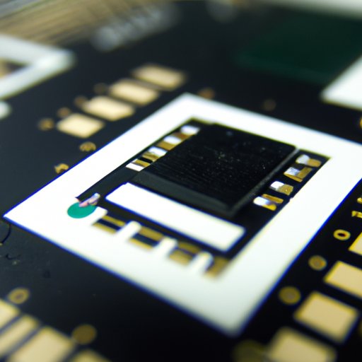
A PCB consists of several basic components, which include a substrate, copper layers, and solder mask. The copper layers are arranged on the substrate, which acts as the base for the components and conductive pathways. The solder mask protects the copper layers from oxidation, eases assembly, and offers mechanical support.
The PCB design process follows these essential steps: schematic design, circuit board layout, and assembly. You start by developing a schematic diagram that identifies the electrical connections between components. Then, the circuit board layout involves arranging the necessary components and traces on the board substrate. Finally, the assembly process involves attaching the components to the board, which includes soldering them to their respective pads.
The History and Evolution of Printed Circuit Boards
The foundation for modern PCBs was laid in the early 20th century when companies started using metal plates and screws to secure vacuum tubes. The advent of radio in the 1920s increased the need for more compact and efficient wiring boards. In the 1940s, the U.S military began experimenting with PCBs, using them in proximity fuses and radios.
Subsequently, in the 1950s, the development of the through-hole PCB technology and the use of double-sided PCBs marked a significant milestone in PCB technology. The invention of computer-aided design(CAD) in the 1960s simplified the design process, making PCBs more reliable, efficient, and cost-effective.
In the 1970s, the introduction of surface-mount technology(SMT) and multilayer PCBs revolutionized the industry, paving the way for compact and more advanced electronic devices. The optimization of PCB manufacturing processes led to the proliferation of electronic devices in the 1980s, which drove up PCB demand and the industry’s growth.
How PCB Technology Has Revolutionized the Electronics Industry
PCB technology brought several advantages that transformed the electronics industry. PCBs are durable and reliable, significantly reducing electronic failures during manufacturing and use. They allow for faster assembly, as components can be easily placed and soldered onto the board. Furthermore, PCBs offer efficient use of space, making it possible to build smaller and more compact devices.
The use of PCBs has had a significant impact on product development and manufacturing processes. PCBs have enabled manufacturers to produce electronic devices faster, with improved quality, and at lower costs. PCBs have contributed significantly to the evolution of modern electronics by offering the possibility of producing more advanced, smaller, and powerful devices.
Examples of electronic devices that use PCBs are ubiquitous. From smartphones and computers to TVs and cars, PCBs provide the foundation on which electronic devices are built. The IoT sector is driving the demand for PCBs further up with new applications such as wearables, smart home devices, and electric cars.
The Anatomy of a PCB: Understanding its Components and Design
The three main components of a PCB are the substrate, copper layers, and solder mask. The substrate is made of a non-conductive material, commonly fiberglass or ceramic, over which copper layers are laminated. The copper layers provide the conductive pathways and interconnects the components.
The solder mask is a protective layer that is applied over the copper traces, except for the electrical contact points. It protects the copper from exposure to the environment, eases the assembly process, and offers mechanical support.
Design considerations for a PCB include layer stacking, trace routing, and via placement. Layer stacking involves deciding how many layers will be used in the PCB and their arrangement to maximize signal quality, reduce interference, and minimize cross-talk between traces.
Trace routing defines the path that the traces will follow on the board. The routing should aim to reduce the distance between components and reduce the impact of interference. Via placement is another critical aspect of PCB design where the design team decides where and how many vias to use to route signals between layers.
PCB layout optimization is crucial in ensuring the design meets the functional and operational requirements of the electronic device. Proper optimization can bring benefits such as increased signal integrity, reduced noise and interference, and reduced manufacturing costs.
PCBs vs. Wire Wrapping: Pros and Cons for Electronic Designers
When it comes to designing electronic circuits, there are several methods to choose from, with PCBs and wire wrapping being the most common. The choice of method depends on various factors such as cost, design complexity, and device performance requirements.
PCBs offer many advantages over wire wrapping. First, they are more reliable and durable, as they use interconnects that are firmly attached to the board. Second, PCBs are much faster and more efficient to manufacture than wire wrapping. Lastly, PCBs allow for more complex wiring schemes, making them suitable for situations that require more intricate circuitry.
The main advantage of wire wrapping is cost. Wire wrapping is cheaper than PCB fabrication since it requires fewer materials and uses less expensive tools. Additionally, prototypes of simple wire-wrapped circuits can be built quickly and inexpensively, making wire-wrapping a common method for testing ideas.
Therefore, the choice of method depends on cost, performance considerations, and design complexity. PCBs are the better option for complicated designs requiring performance, durability, and efficiency, while wire wrapping is suitable for simple testing prototypes that do not need a longer life-span and high reliability.
The Future of PCB Technology: Trends and Predictions
The future of PCB technology is bright, with several emerging technologies shaping the future. New manufacturing processes such as 3D printing, in-circuit test, and surface-mount assembly are enabling faster and more efficient production. New materials such as flexible substrates, conductive polymers, and graphene are paving the way for more versatile and robust PCBs.
PCBs are becoming more integrated and capable, offering a higher degree of functionality than ever before. The integration of sensors, Intelligent power-management systems, and wireless communication technologies into PCBs is expanding the range of applications, ranging from medical to automotive, industrial, and military sectors.
The growth of the IoT sector is also driving the demand for PCBs, as the need to connect and communicate smart devices increases. The future of PCB technology looks bright, with new materials, fabrication methods, and applications continually emerging.
How to Choose the Right PCB Manufacturer for Your Project
Choosing the right PCB manufacturer is an important decision that can dramatically impact the functionality and reliability of your electronic device. In this section, we will discuss some vital factors to consider when choosing a PCB manufacturer.
First, consider the quality of the manufacturer’s products. The manufacturer’s capabilities in designing, fabricating, and assembling PCBs have a direct impact on the quality of the circuits produced. A reliable PCB manufacturer should demonstrate its quality through certifications such as ISO 9001 or UL.
Second, consider the manufacturer’s lead time and the production capacity. You should choose a manufacturer that can provide you with PCBs when you need them for your project. Manufacturers that have large production capacities are better suited for bulk orders, requiring faster delivery times.
Finally, consider the price of the PCBs and the manufacturer’s ability to provide timely support. You should choose a PCB manufacturer that offers affordable and competitive prices without compromising on quality. Furthermore, consider the quality of the manufacturer’s customer service and technical support when making your decision.
Conclusion
PCBs are an integral part of the modern electronics industry, offering several advantages over conventional wired assemblies. They are durable, efficient, and cost-effective, making them a popular choice for many electronic devices. Understanding the basics of PCB design and manufacturing is essential for electronic engineers and enthusiasts alike.
The evolution of PCB technology has brought significant benefits to the electronics industry, fueling the development of more advanced, durable, and efficient electronic devices. The future of PCB technology looks bright, with emerging technologies paving the way for more versatile, reliable, and cost-effective PCBs.
When choosing a PCB manufacturer, it is crucial to consider factors such as quality, production capacity, and price, alongside timely support. Choosing the right PCB manufacturer can make a significant difference in the success of your electronic device design and manufacturing.